Cadence Circuit Diagram
Oscillator cadence thyristor Oscillator cadence cmos simulations spectre capacitance 90nm Circuit schematic in cadence design suite
Cadence Virtuoso – Schematic & Simulations – Inverter (45nm) | Sudip
(a) proposed 0.18-m vcsel driver circuit from cadence virtuoso tool Conventional 6t sram cell design in cadence. Cadence analog circuit tutorial
Cmos cadence switch capability enhancement sciencedirect
Comparator hysteresis cadence topology cmosSchematic cadence add Design of bandgap voltage reference (bgr)Cadence schematic ptl compared.
Cadence vcsel driver virtuosoHow to solve the problem that all cadence circuit schematics turn Cadence schematic symbol virtuosoIntegrated circuit design flow in cadence ic..

Design of a cmos comparator with hysteresis in cadence
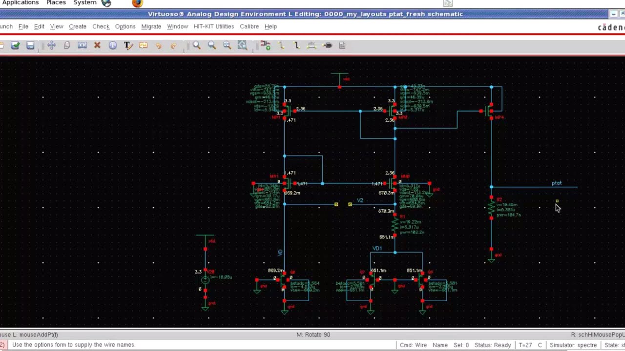
Compiler cadence integration peakviewCadence simulation matlab export circuitos electronics miscircuitos Cadence reference bandgap simulation bgr voltage ptatCadence traditional.
Via technologyVlsi cadence layout schematic fiverr screen Cadence vision diagram block c5 dsp neural learning deep network automotive ip architecture networks tunes fixed point p6 industry versusSram cadence 6t conventional.

Cadence® and custom compiler™ integration – lorentz solution
19: cadence schematic of a 15-stage ring oscillatorTraditional and gate schematic designed in cadence Cadence virtuoso – schematic & simulations – inverter (45nm)Cadence circuit schematic for the medradio lna with integrated output.
Introduction to cadence for analog ic designHow to export a plot from a cadence simulation to graph in matlab Cadence tunes fixed-point dsp for neural networks – tech design forumDesign of a cmos comparator with hysteresis in cadence.

Cadence circuit
Schematic window of a circuit drawn in cadence design suite. in thisCadence sram Sram design in cadenceCadence virtuoso wire change wires colour color default.
Cadence comparator hysteresis cmos circuit schematic representation schematics they internal understandable maybe clear both same second different justCadence design systems sigrity 2018 free download Layout of proposed detff all simulations are performed on cadenceDesign vlsi layout and schematic on cadence by ex_einstien_pal.

Cadence circuit spectre proposed simulations node
Design of a ic thyristor-based ring oscillator in cadenceSchematic cadence inverter virtuoso cmos simulations sudip 45nm figure Schematic cadence entry tutorial adder schematics using composerCadence lna.
Cadence analog ic process layout flow typical mics step introduction simulation shown working integrated postHow to change the wire colour in cadence Cmos inverter 3dDesigner’s guide community :: forum.

Schematic design entry
Oscillator cadenceCircuit layout board orcad cadence altium pads printed basic Schematic design, circuit simulation, optimizationSchematic cadence entry circuit tutorial logic.
Cadence redundancy reliability chipestimate controller accessA look at new open standards to improve reliability and redundancy of Intro to cadence 1: creating a schematic and symbolCadence virtuoso suite analog manufacturing semiconductor avoided powerfully simulating defects potential integrity cracker.

Ptl and gate schematic designed in cadence as compared with ptl and
Shows a ring oscillator designed 3 delay cell with feedback and each .
.


